
QuantumDiamonds chip inspection has moved from quantum demo to EU-backed industrial bet, with €76 million in approved public funding and a fresh €15 million equity round aimed at turning diamond-based sensors into fab-floor equipment.
XOOMAR Intelligence
Analyst Take
The German startup, a spinout from the Technical University of Munich, will use the state-backed funding to build a semiconductor testing equipment facility in Munich as part of a previously announced $178 million investment plan, according to TechCrunch. The round was led by World Fund, with backing from Bayern Kapital and existing investors including Creator Fund, Earlybird, First Momentum, IQ Capital, Onsight Ventures and UnternehmerTUM.
Why chipmakers care about QuantumDiamonds chip inspection now
The thesis is simple: making more chips only helps if manufacturers can find defects fast enough to keep output high. That is where QuantumDiamonds chip inspection is trying to wedge itself into the semiconductor production chain.
The company claims its system can compress a defect detection process that usually takes weeks into a two-minute inspection that does not stop production lines. CEO Kevin Berghoff told TechCrunch this could help Taiwan-based foundries and Korea’s memory makers save hundreds of millions of dollars. He also said the hardware is typically paid back within a couple of months.
That claim matters because QuantumDiamonds is not trying to replace lithography. It sits in the inspection and metrology layer: the tools that help manufacturers understand whether a chip or advanced package is behaving as intended. Europe already has ASML, the Dutch supplier with a near-monopoly in the machines used for chipmaking. But one champion does not make a full semiconductor toolchain.
The counterpoint is obvious. Semiconductor fabs are conservative buyers. A tool that looks promising in a lab still has to prove it can survive production conditions, integrate with existing workflows, and justify its price. QuantumDiamonds’ case will stand or fall on measurable factory gains, not on quantum branding.
“They couldn’t care less about it being quantum,” Berghoff told TechCrunch.
QuantumDiamonds is selling defect visibility, not quantum mystique
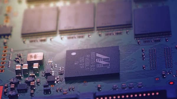
QuantumDiamonds’ real product is visibility into hidden electrical behavior inside chips. The company uses synthetic diamonds with engineered atomic-scale defects known as nitrogen-vacancy centers. These centers react to magnetic fields. Since electrical current generates magnetic fields, the system can map how electricity flows through a semiconductor device.
That is different from current inspections described by TechCrunch as looking at the top layer of a chip with “a microscope of sorts.” QuantumDiamonds says its method can detect defects through all layers without destroying the chip. That becomes more relevant as chips become more multi-layered.
Berghoff framed the problem bluntly:
“The thing is that the transistors cannot get smaller, so in order to get the same power and the same compute, you start to add more and more layers.”
This is the same pressure showing up across AI infrastructure. XOOMAR has covered the demand side in Banks Hand Nscale $900M as AI Compute Race Turns Real, while semiconductor supply strategy is also showing up in deals like Apple Broadcom Deal Pulls $30B Chip Bet Back to U.S.. QuantumDiamonds is attacking a narrower but critical bottleneck: finding faults inside the chips and packages that feed that demand.
How diamonds spot defects conventional tools can miss
The strongest technical claim is non-destructive, layer-penetrating current mapping. According to related reporting from Move the Needle, QuantumDiamonds’ technology has been evaluated through proof-of-concept projects with nine of the world's ten largest semiconductor manufacturers. The European Commission described the planned Munich site as Europe’s first production facility for semiconductor metrology and inspection systems based on quantum sensing technology.
The basic mechanism is not sci-fi. The diamond sensor reads magnetic fields created by current inside a chip. Software then interprets that data and gives customers an indication of what they should address in the manufacturing process, according to TechCrunch.
Here is the contrast:
| Inspection approach | What the supplied sources say | Core trade-off |
|---|---|---|
| Top-layer microscope-style inspection | Looks at the top layer of a chip | Limited visibility into buried defects |
| Thermal or X-ray tools | Standard tools may miss some hidden faults, according to Dr David Su quoted by Move the Needle | Useful, but not always enough for advanced packages |
| Quantum Diamond Microscopy | Maps current via magnetic fields using synthetic diamonds | Promising, but must prove production-grade reliability |
The hard part is not the physics alone. It is industrialization. QuantumDiamonds already has a lab tool for sample-based testing, where customers may test “one out of a million chips,” Berghoff said. The next target is high-throughput testing that could support 100% quality control in the fab itself.
The two-minute claim is the business case
If QuantumDiamonds can really turn weeks of defect detection into two minutes, the economics become easier to understand. The company says its inspection does not stop production lines. That point is central, because downtime and slow diagnosis are poison in semiconductor manufacturing.
Use the company’s own migration path as the example. Today, Berghoff says QuantumDiamonds has a tool for a lab environment, used for sample-based testing. The planned high-throughput system is meant to move from clients’ labs into their fabs. That shift changes the role of the tool from occasional investigation to routine quality control.
The prices also show where QuantumDiamonds wants to sit. Berghoff said lab tools are in the single-digit millions, while a high-throughput system could cost $10 million to $15 million. He compared that with ASML machines that may cost $400 million.
Analysis: That comparison is not saying QuantumDiamonds is the next ASML in scale today. It says the startup is selling into a cost structure where a multimillion-dollar tool can still be “quite cheap” if it shortens diagnosis and protects output at large fabs. The claim that customers can recover the cost within a couple of months is the one investors and chipmakers will test hardest.
Why Europe is backing more than ASML
The EU angle is industrial policy aimed at the equipment stack, not just chip production. The European Chips Act aims to support the semiconductor industry partly through state subsidies. QuantumDiamonds is one of the beneficiaries, with funding provided by Germany’s federal economy ministry and the state of Bavaria after European Commission approval.
A separate eeNews Europe report said the aid is a direct grant for the company’s IPF-ATEST project. It also reported that QuantumDiamonds has committed to collaborating with universities and research institutes, expanding the skilled semiconductor workforce, making part of the facility available to startups, SMEs and academic labs, prioritizing customer orders during semiconductor supply shortages, and sharing project-related profits with Germany if returns exceed expectations.
That makes the funding more than a startup subsidy. It is a bet that Europe needs more control over the tools used to verify chips, not only the tools used to print them.
World Fund managing partner Daria Saharova went further, writing that QuantumDiamonds “can become Europe’s next ASML.” That is venture capital optimism. Berghoff was more candid, telling TechCrunch that ASML could also be a possible acquirer someday, while noting ASML recently said it is not too keen on M&A.
The fab-floor test will decide whether the hype holds
QuantumDiamonds has three hurdles: throughput, trust and incumbents. The startup says it has completed first commercial deployments in Taiwan and the U.S., including a system at Eurofins EAG Laboratories in Sunnyvale, California. It also opened a regional hub in Taiwan. Those are useful proof points, but the bigger challenge is moving from customer labs into production fabs.
Established inspection companies already have customer relationships and product portfolios. Berghoff argues QuantumDiamonds has a first-mover advantage, saying: “There is no U.S. or Asian company that has shipped those tools.” That advantage only matters if the tools perform repeatedly under fab constraints.
The Munich facility will also test whether European support can turn deep-tech research into exportable industrial equipment. Most of QuantumDiamonds’ 70-person team is based in Munich, and Berghoff and co-founder and CTO Fleming Bruckmaier plan to double the engineering team over the next 12 months.
The practical watch item is narrow but decisive: can QuantumDiamonds show that diamond quantum sensing produces faster defect detection and better factory decisions at production scale? If yes, the EU gets a new semiconductor equipment contender. If not, this remains a well-funded lab-to-fab experiment with impressive physics and a harder commercial path.
Impact Analysis
- Faster defect detection could help chipmakers improve output without adding new fabrication capacity.
- EU backing signals a push to build more of the semiconductor equipment chain in Europe.
- QuantumDiamonds still faces the challenge of convincing conservative fabs to adopt new inspection hardware.
Chip Defect Inspection Approaches
| Traditional inspection | QuantumDiamonds approach |
|---|---|
| Can take weeks to detect defects | Claims inspection can be done in two minutes |
| May slow production analysis cycles | Designed not to stop production lines |
| Established fab process with conservative buyers | New diamond-based sensor system seeking fab-floor adoption |
QuantumDiamonds Funding
Primary Sources & Disclosures

Written by
XOOMAR Insights Team
Research and Editorial Desk
The XOOMAR Insights Team pairs automated research with human editorial judgment. We track hundreds of sources across technology, fintech, trading, SaaS, and cybersecurity, cross-check the facts, and explain what happened, why it matters, and what to watch next. We do not just rewrite headlines. Every article is fact-checked and scored for reliability before it goes live, and we link back to the original sources so you can verify anything yourself.